


high speed pcb -pcb board manufacturer from China
B1003
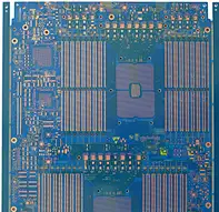
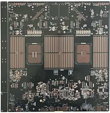
High speed digital board Ultra large size High speed communication backplane
Quantity
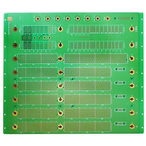
▪ Number of layers -26L
▪ Material - Tachyon 100G, hydrocarbon
▪ Plate thickness -3.5 ± 0.35mm
▪ Inner and outer copper thickness -0.33OZ
▪ Minimum line width/line spacing -0.118/0.051mm
▪ Minimum aperture -0.225mm
▪ Surface Treatment - Gold Deposition
▪ Application Field - Industrial Control Systems
What issues should be noted in high speed design ?
high speed pcb design guidelines are as follows:
high speed pcb design guidelines are as follows:
1、 The Influence of Wiring Topology on Signal Integrity
Signal integrity issues may arise when signals are transmitted along transmission lines on high-speed PCB boards.
2、 The influence of solder pads on high-speed signals
In PCB, from a design perspective, a through hole mainly consists of two parts: the drilling hole in the middle and the solder pad around the drilling hole.
3、 How to suppress electromagnetic interference
PCB is the source of electromagnetic interference (EMI), so PCB design is directly related to the electromagnetic compatibility (EMC) of electronic products.
4、 Whether to choose through hole or bent RF wiring
Analyzing the return path of RF circuits is different from signal return in high-speed digital circuits. The two have something in common, both are distributed parameter circuits that use Maxwell's equations to calculate the characteristics of circuits. But RF circuits are analog circuits, where both voltage V=V (t) and current I=I (t) variables need to be controlled, while digital circuits only focus on changes in signal voltage V=V (t). Therefore, in RF wiring, in addition to considering signal return, it is also necessary to consider the impact of wiring on current.