

Multilayer HDI PCB-FPGA Development Board Core Board
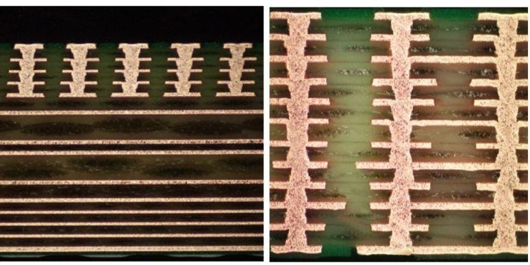
Multilayer circuit boards, on the other hand, are printed boards comprising several layers of insulating substrates and connecting wires alongside solder pads. With their unique insulating properties, these boards conduct circuits on each layer, while providing mutual insulation. Taking Huawei MateBook X and Win10 as examples, HDI boards are typically produced using the stacking method, which involves using multiple layers to increase the board's technical level. Higher-order HDIs employ advanced PCB technologies such as hole stacking, electroplating filling, and laser direct drilling to achieve more than 2 layers. When the density of the PCBs exceeds eight layers, using HDI technology results in lower manufacturing costs compared to traditional complex pressing processes.
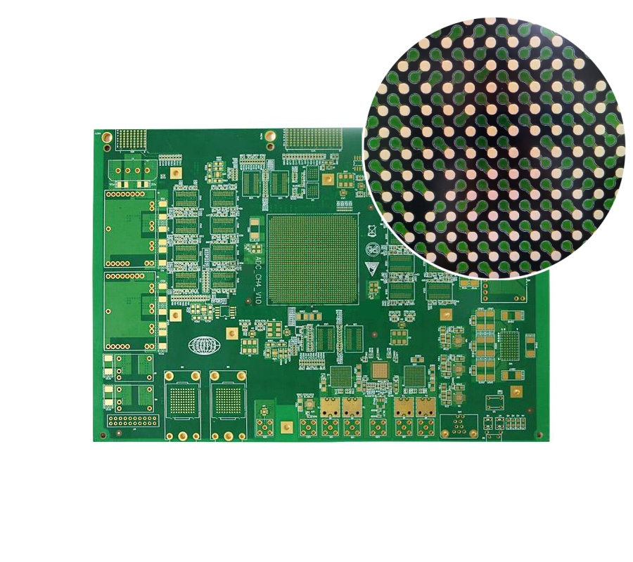
2.Your PCB board impedance will be controlled within plus or minus 8%. For multi-layer BGA, the export wiring rules involve wiring trajectories through multiple rows of pins, some of which may carry high-speed signals, and we will be able to control the impedance within plus or minus 8%.
3.Your HDI (High Density Interconnect) board will be produced at a high level of craftsmanship. As the pin spacing decreases, the required wiring width to reach each layer of BGA between pins will become smaller and smaller. For controlled impedance signals, this means that you will need thinner laminates and ultimately HDI technology. HDI boards are BGABOARD's advantageous process and have extensive experience in the following processes: Depth control drill POFV, resin plug hole plate, (Any layer HDI), POFV (VIPPO) blind/bored hole plate, plate over filled via.
Why can we make BGA high multilayer PCB boards? This is because of our years of production experience, strict data processing, high-end processing equipment, and comprehensive shipment testing, which enable each PCB to meet the most perfect standards.