What is PCB Via In Pad(VIP)?
What is PCB via in pad(VIP)?
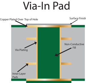
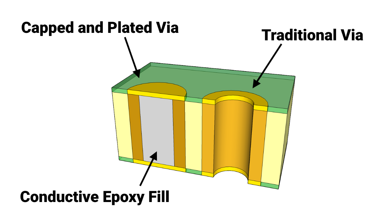
PCB via in pad (VIP) refers to the PCB surface pad containing via holes. In PCB design, via in pad (VIP) technology is widely used in PCBs with limited BGA space.The via holes on the BGA are generally defined as PCB via in pad (VIP) in the plate and need to be plugged with resin. The resin is electroplated and capped to facilitate customer soldering. Except if the customer requires that the holes on the BGA should not be plugged. Except for BGA, when the customer requires all vias to be plugged with resin, the vias on the patch are also defined as PCB via in pad (VIP).

BGABoard pcb via in pad
The windows of the BGA solder joints are displayed in a square array, arranged neatly, and the via holes are drilled on the BGA solder joints to avoid errors in judgment caused by the opening of the via holes.
In the BGA area, pay attention to the size of the solder mask, patch, and solder flux windows, because the actual size of the circuit layer pads shall prevail. Don't just think that it is a hole in the plate when you see the window hitting the hole.
Don't mistake PGA as a hole in the plate: customers need to insert pin corners in the PGA area. Generally, the pad area or solder ring is relatively large. Please refer to the customer's instructions.This hole is 0.2mm, the patch layer has a window, and the circuit pad is 12mil. Based on the size of the pad, drilling, and characters, the patch can be determined to be a hole in the plate.
For some smaller holes on ordinary PCB boards where parts need to be soldered, the traditional production method is to drill a through hole on the board, and then plate a layer of copper in the through hole to achieve conduction between layers (as shown below) 1), and then lead a wire to connect a pad to complete the welding with the external parts (Figure 1)

BGABoard Specialize In BGA Board Manufacturing.

Why do PCB via in pad?
Nowadays, PCB circuit boards are becoming more and more high-density and interconnected, and there is no more space to place the wires and pads connecting the through holes. Therefore, under this background, the production process of PCB via in pad was born.


Vias In Pad Design
Pad In Via Design