Pad In Via Design
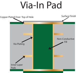
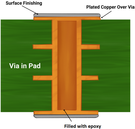
The definition of Pad In Via refers to the Via under the pad.
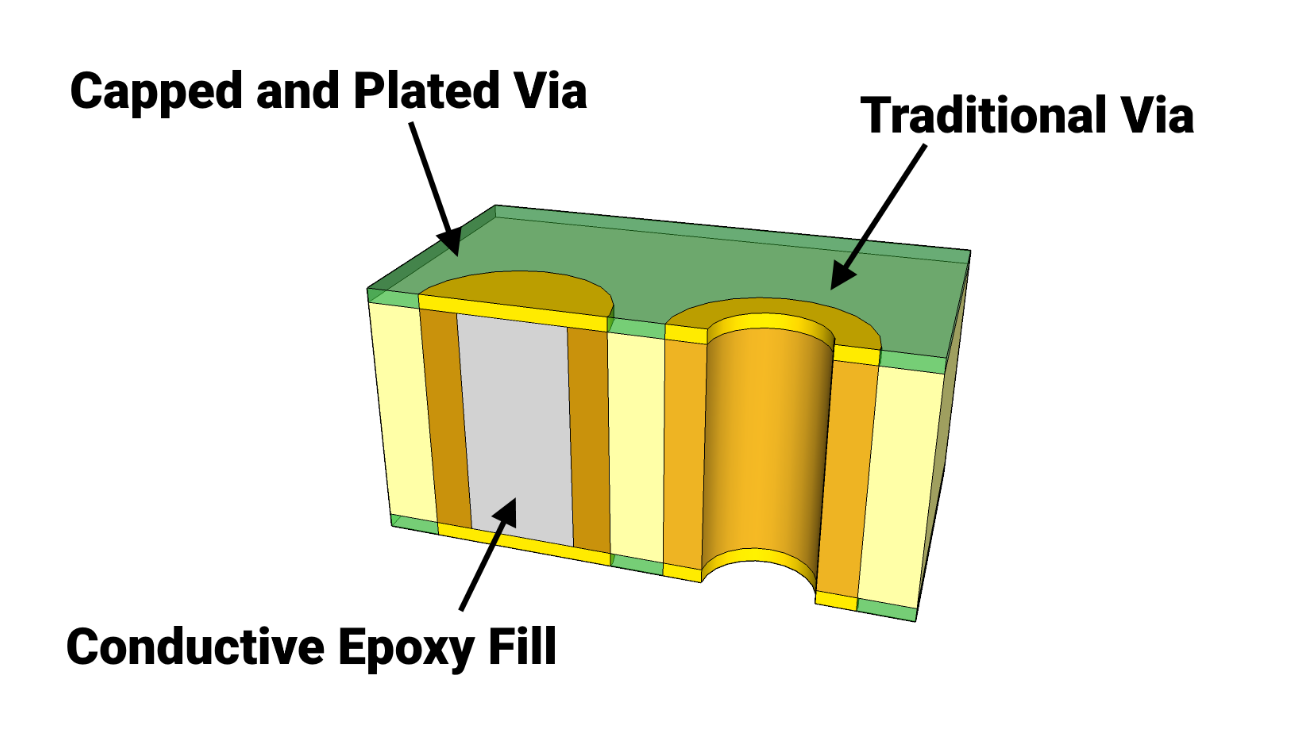
After the inner diameter of the pad passes through the resin plug hole, a layer of copper is electroplated on the inner diameter base material to make the surface look like a large copper surface, and the hole is buried under the pad.
Pad In Via can increase the surface pad area. For small line width and line spacing, PCB wiring, and small pad area, it can reduce the area and reduce the size of the PCB while completing the conductivity.
Pad In Via can increase the surface pad area. For small line width and line spacing, PCB wiring, and small pad area, it can reduce the area and reduce the size of the PCB while completing the conductivity.
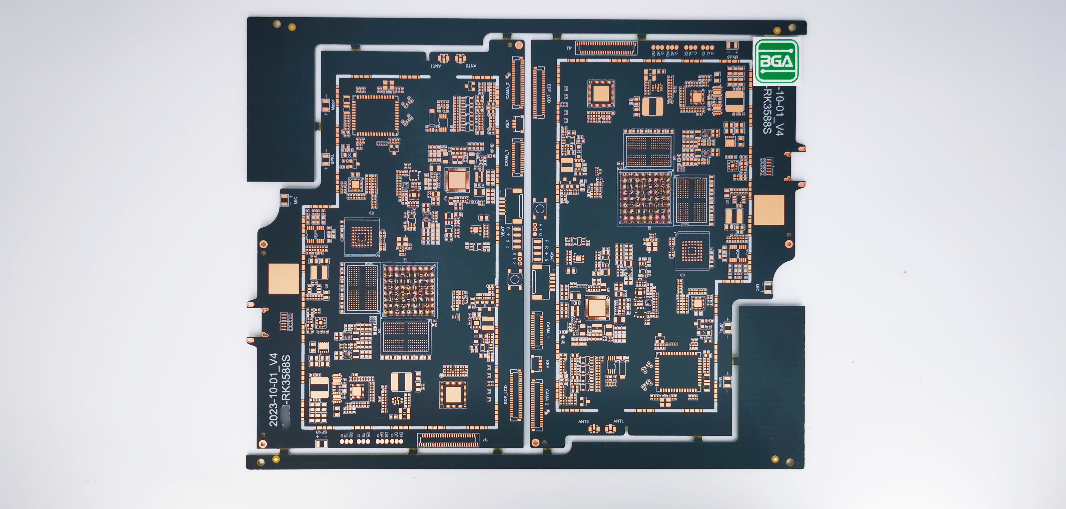
BGABoard pad in via printed circuit board
As electronic products develop in the direction of being light, thin, and small, PCB boards are also pushed towards high-density and difficult development, so the size of components is gradually becoming smaller. For example: the package of BGA components is small, and the pitch of the pins becomes smaller. If the pin spacing is small, it is difficult to route the pins inside the package, and it is necessary to change layers and drill holes for routing.
The first feeling that in pad via brings to LAYOUT engineers is that it is "silky", and they can finally drill holes on the pads and BGA at will; the second is efficiency, pad in via process can greatly shorten the wiring time, which was originally possible What took 7 days now only takes 2 days. In the extra few days, I can draw two more boards.
Even if the via hole is not drilled on the pad, the performance and effect of pad in via process are far better than "via cover oil" and "via plug oil". There is neither the problem of yellowing of the oil hole of the via cover nor the problem of poor SMT welding performance caused by the easy leakage of oil from the via plug.
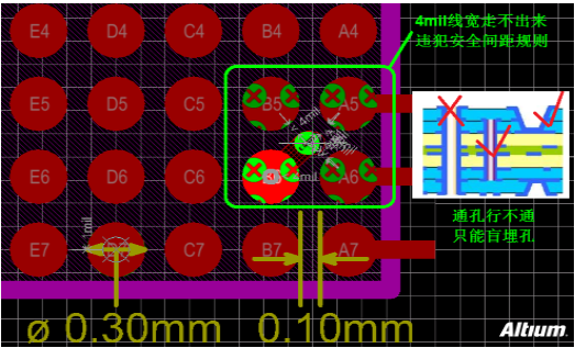
As shown in the picture above,The minimum line width is 0.1mm (4mil), the minimum safety spacing is 0.1mm (4mil), and the minimum laser aperture is 0.1mm (4mil). We won’t consider mechanical drilling either, as the laser holes won’t even fit!
The thread can't come out! ——Solution: Blind and buried hole drilling instead of through holes.
The thread can't come out! ——Solution: Blind and buried hole drilling instead of through holes.
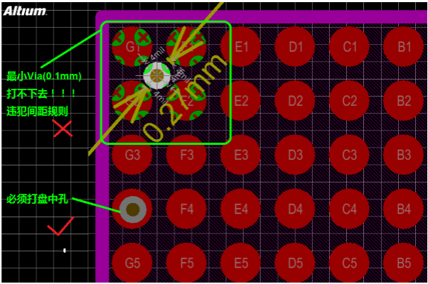
There is no place to punch Pad In Via! ——Solution: Pad In Via
As shown in the picture above, the minimum laser hole of 0.1mm (4mil) cannot be drilled between the pads because the maximum diagonal distance between the edges of the pads is 0.27mm. Even the smallest hole drilled in the middle cannot meet the safety rule of the minimum spacing of 4 mil. Therefore, only the center hole can be drilled. However, the process of Pad In Via is complicated and requires subsequent processing, such as filling and plugging the holes, adding electroplating, smoothing the surface and other processes. Processing costs will also increase accordingly.
Conclusion on wiring solutions for extremely small BGA (0.4mm pitch) devices:
Technically, only multilayer board wiring with more than 4 layers can be carried out. BGA devices have a 0.4mm ball spacing and a 0.3mm ball pad diameter. Laser blind holes are required for interconnection (the minimum laser processing aperture capability is 0.1mm). It is possible to make 2-level interconnections according to design requirements; and Pad In Via design is required. .
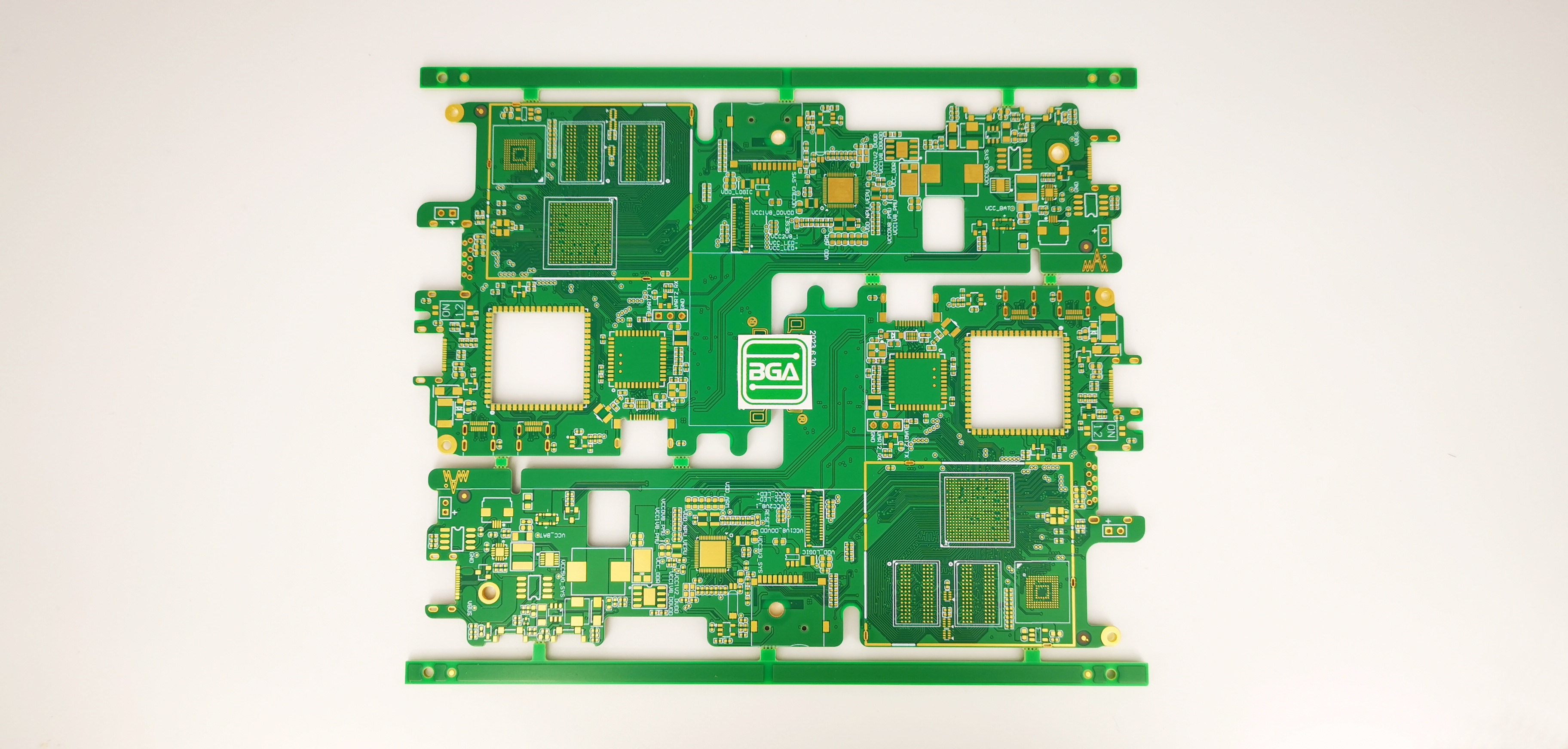
BGABoard in pad via printed circuit board
What is PCB Via In Pad(VIP)?