Vias In Pad Design
Vias In Pad Design
1. No need to design Vias In Pad
Before conducting PCB wiring, it is necessary to perform fan out work to facilitate internal wiring. For BGA type devices, the number of pins is too large, and the BGA interval must have the fan hole in the center position between the pads. Regarding the setting parameters for BGA fanout, the through-hole is 0.15-0.2mm, the line width is 3-4 mils, and the hole ring is 0.3-0.4mm. Therefore, the BGA pin spacing needs to be greater than 0.35mm in order to fanout normally.
Before conducting PCB wiring, it is necessary to perform fan out work to facilitate internal wiring. For BGA type devices, the number of pins is too large, and the BGA interval must have the fan hole in the center position between the pads. Regarding the setting parameters for BGA fanout, the through-hole is 0.15-0.2mm, the line width is 3-4 mils, and the hole ring is 0.3-0.4mm. Therefore, the BGA pin spacing needs to be greater than 0.35mm in order to fanout normally.

2. Need to design Vias In Pad
Before BGA fanout, we need to set Vias In Pad of the via hole, otherwise the aperture is not suitable and cannot be effectively fanout, or the fanout result is abnormal. When the spacing between BGA pins is too small to fan out, it is necessary to design Vias In Pad to route wires from the inner layer or the bottom layer of the BGA device.
Before BGA fanout, we need to set Vias In Pad of the via hole, otherwise the aperture is not suitable and cannot be effectively fanout, or the fanout result is abnormal. When the spacing between BGA pins is too small to fan out, it is necessary to design Vias In Pad to route wires from the inner layer or the bottom layer of the BGA device.

1) Vias In Pad on BGA
Generally, there is no need to design holes in the disk for packaging devices with fewer pins. BGA devices have more fanned vias that occupy wiring space. If the vias are designed as Vias In Pad and punched on the BGA pad, space for wiring can be reserved. When the pin spacing is too small for wiring, holes in the disk can be designed and wiring can be done from other layers.
2) Vias In Pad on filter capacitor
When routing within BGA devices requires many through holes, it is difficult to avoid through holes by plugging filter capacitors on the back of BGA devices. Therefore, through holes are punched on the solder pad, becoming Vias In Pad.

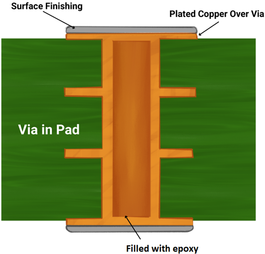
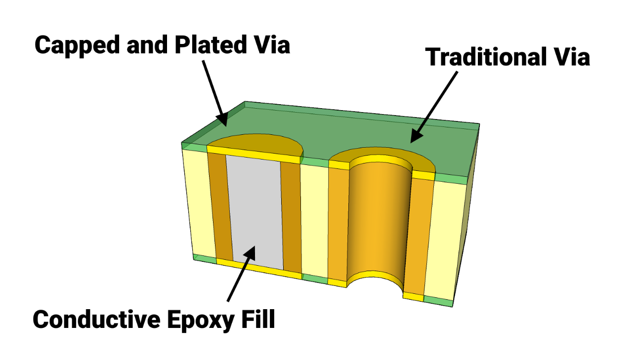
You can use a solder mask layer as a sealing medium to prevent solder from being sucked into the through-hole cavity, which is a traditional method. For VIP structures, a fully filled through-hole cavity is required to eliminate stagnant air and degassing, and a precise and flat plane is also required to reliably connect fine spaced BCAs.
The manufacturing options available for VIP include mechanical drilling, electroplating, and non-conductive epoxy resin filling methods, as well as laser ablation and all copper filling methods for Vias In Pad.
The manufacturing options available for VIP include mechanical drilling, electroplating, and non-conductive epoxy resin filling methods, as well as laser ablation and all copper filling methods for Vias In Pad.

3. Design of common Vias In Pad
1) BGA pad with Vias In Pad
2) QFN device solder pads with holes in the disc
3) Through holes exist on component pads, such as resistors or capacitors
4) Through holes located within IC pads or connectors or multi pin components
In some cases, it is not necessary to fill the vias. For example, thermal conductive pads do not need to be welded because they do not need to be considered as Vias In Pad.
4. Vias In Pad that do not require solder filling
1) Thermal conductive pads that do not require solder filling
2) Through holes not on pads
When no vias are actually placed on the pad, there is no need to fill the vias.
1) BGA pad with Vias In Pad
2) QFN device solder pads with holes in the disc
3) Through holes exist on component pads, such as resistors or capacitors
4) Through holes located within IC pads or connectors or multi pin components
In some cases, it is not necessary to fill the vias. For example, thermal conductive pads do not need to be welded because they do not need to be considered as Vias In Pad.
4. Vias In Pad that do not require solder filling
1) Thermal conductive pads that do not require solder filling
2) Through holes not on pads
When no vias are actually placed on the pad, there is no need to fill the vias.
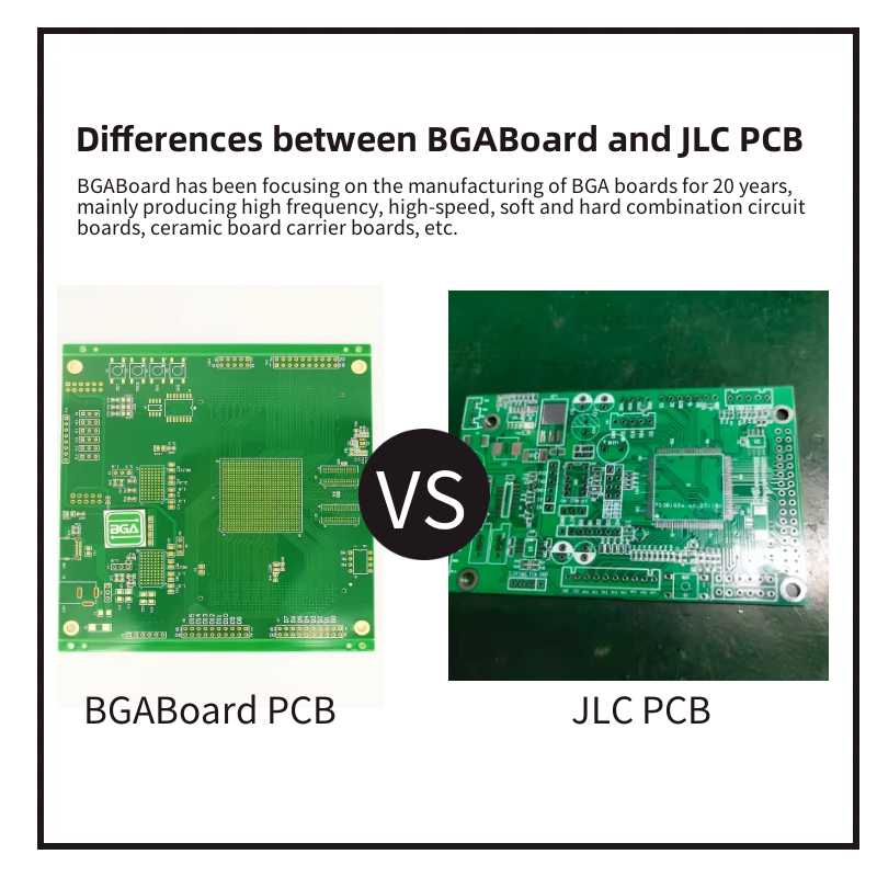
What are the differences between the circuit boards of BGABoard and JLC PCB?
What is PCB Via In Pad(VIP)?